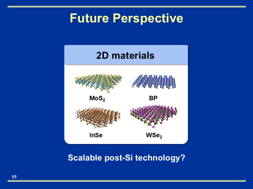
This video article highlights the recent works by Prof. Kaihui Liu’s group at Peking University in making wafer-scale 2D semiconductor thin films. In contrast to conventional epitaxial surface growth methods, they have developed two novel epitaxial interface growth methods, which have enabled them to make various 2D semiconductors in wafer scale for device fabrication. As exemplified in this video highlight, using the novel interfacial lattice-epitaxy growth method, they have successfully made single-crystal 4-cm wafers of MoS2, with a thickness ranging from 1 to ~1500 layers, of high crystallinity and uniformity. Furthermore, they fabricated mono-, bi-, and tri-layer MoS2 transistors, whose electrical performance exceeds the IRDS 2028 mobility target. Also, using the interfacial solid-liquid-solid growth method, they have made single-phase single-crystal 5-cm wafers of InSe multilayer films and fabricated integrated circuits of transistor arrays with a performance matrix surpassing the Si Intel 3nm technology.
1. B. Qin, C. Ma, Q. Guo, X. Li, W. Wei, C. Ma, Q. Wang, F. Liu, M. Zhao, G. Xue, J. Qi, M. Wu, H. Hong, L. Du, Q. Zhao, P. Gao, X. Wang, E. Wang, G. Zhang, C. Liu, and K. Liu, Interfacial epitaxy of multilayer rhombohedral transition-metal dichalcogenide single crystals, Science 385, 99 (2024).
2. B. Qin, J. Jiang, L. Wang, Q. Guo, C. Zhang, L. Xu, X. Ni, P. Yin, L.-M. Peng, E. Wang, F. Ding, C. Qiu, C. Liu, and K. Liu, Two-dimensional indium selenide wafers for integrated electronics, Science 389, 299 (2025).
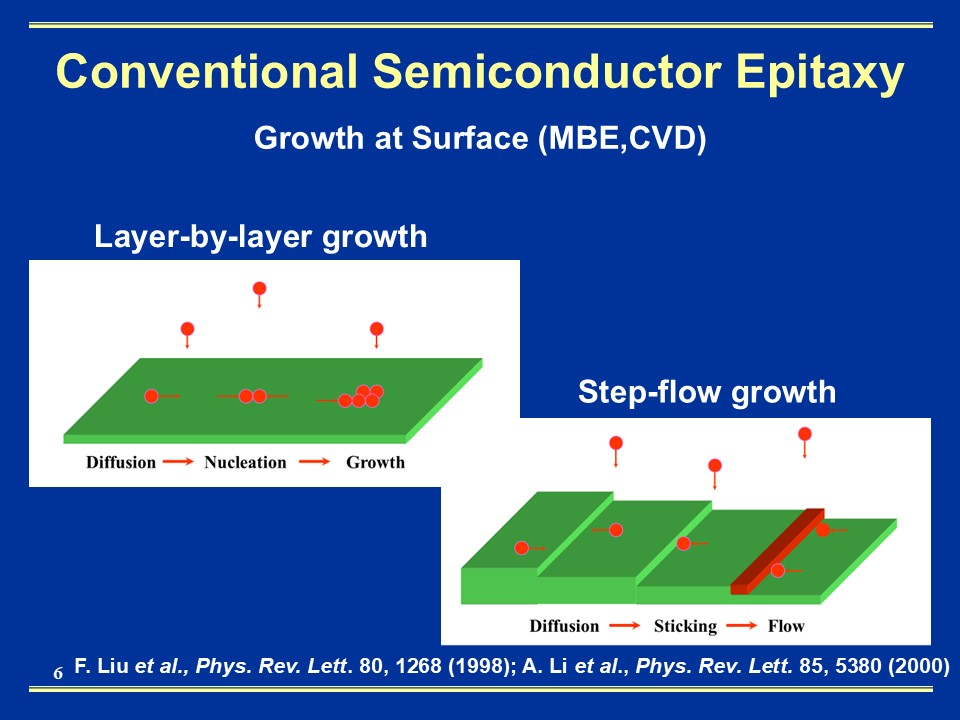
3. F. Liu, J. Tersoff, and M.G. Lagally, Self-organization of steps in growth of strained films on vicinal substrates, Phys. Rev. Lett. 80, 1268 (1998).
4. A. Li, F. Liu, D.Y. Petrovykh, J.-L. Lin, J. Viernow, F.J. Himpsel, and M.G. Lagally, Creation of "quantum platelets" via strain-controlled self-organization at steps, Phys. Rev. Lett. 85, 5380 (2000).

